
Strontium Titanate Single Crystals(Furuuchi Chemical)
Summary
It is possible to control the carrier concentration and transmittance by doping, and this product is expected to contribute as a key device for optical networks with large capacity, ultra-high speed, and low power consumption.
Application Examples
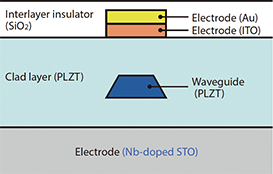
Optical switches with PLZT thin film fabricated on Nb-doped SrTiO3 single crystal substrates can achieve lower control voltage, faster response, and lower polarization dependence, leading to increased capacity, ultra-high speed, and low power consumption of optical networks.
*PLZT:Pb1-xLa(x ZryTi1-y)1-x/4O3
Benefits for Customers
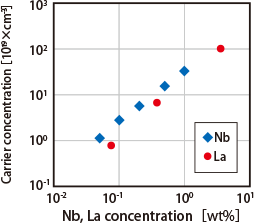
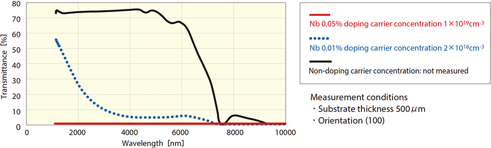
- Carrier concentration and transmittance can be controlled by Nb or La doping.
- Larger crystals with a 2-inch diameter are expected to enable larger devices.
- Crystal growth along with (110) and (111) as well as (100) is achieved.
Features of Strontium Titanate Single Crystals
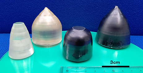
Boules
Doping Amount and Carrier Concentration
Transmittance of STO substrate
FAQ
What sizes are available?
-
The standard size is 10 mm x 10 mm, but we are working on increasing the size by growing large crystals, so please feel free to contact us.
Are Nb and La the only elements that can be doped?
-
Nb and La are the standard, but please contact us to discuss the possibility of doping other elements as well.
Other products related to High-Functional Materials for Next Generation Devices
- Printed Electronics Copper ink
- High-Purity Metals
- Low α Tin/Bismuth for Soft Error Reduction
- Electroless UBM Formation Service
- Compound Semiconductor Wafers - InP, CdZnTe -
- Rutile Single Crystals(Furuuchi Chemical)
- YAG Ceramics for Laser Applications
- Tantalum and Niobium Oxides and Compounds (TANIOBIS)
- AMPERTEC® High-Purity Chlorides(TANIOBIS)
- Photocatalyst for Artificial Photosynthesis
- Sintering Copper Fine Powder