
Introducing JX Advanced Metals' core technologies that contribute to
social development and innovation
Introducing JX Advanced Metals' core technologies that contribute to social development and innovation
-
Purification
Reducing impurities by applying various refining and melting technologies
- Refining
- Melting
-
Precision Rolling
and FabricationThe world's thinnest rolled copper foil, as well as fabrication of ultrafine shaped parts
- Rolling
- Accurate bulk machining
-
Composition and
Microstructure DesignDesign achieving advanced functionality materials
through control at crystal structure level- Design of metals, alloys, and composites
- Ceramics design
- Single crystal growth

-
Powder Design
Producing metal and ceramic powders through control of grain size and other characteristics
- Powder manufacturing
- Powder handling

-
Surface Design
Achieving new functional properties in materials through our own surface control technology
- Polishing, etching, and cleaning
- Surface deposition and plating
- Surface treatment
- Adhesion, bonding, and compositing

-
Analysis and Evaluation
Advanced analytical technology is essential for high-performance, high-quality materials
- Inorganic and organic analysis
- Surface and structural analysis
- In-house evaluation
- Computer-aided engineering and materials informatics
-
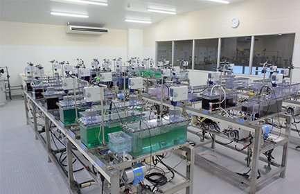
Extraction and Refining
Supporting a Sustainable Society from Resources to Recycling
- Mineral resource exploration and development
- Smelting and refining
- Recycling technologies

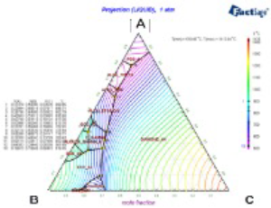
Refining
- Original in-house refining processes (electrorefining, solvent extraction, distillation/sublimation) for various metal raw materials.
- Providing high-purity metals and sputtering targets by combining refining technologies.
Melting
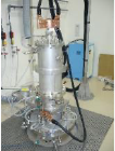
- Since many metals undergo oxidation during melting, we use high-vacuum melting methods such as electron beam melting (EBM) and plasma arc melting (PAM). The optimal melting method for each metal is applied to the manufacture of high-purity metals.
- By combining refining technologies, we provide high-purity metals and high-purity materials such as sputtering targets.
-
- Example of Refining Technology -
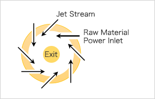
- Molten salt electrolysis method
For metal elements that are not readily electrolyzed in a water solution, a process called molten salt electrolysis can be used for high purification.
-
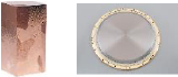
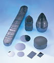
- Typical Product Application -
- 9N Cu
The world's highest purity 9N (99.9999999%) is achieved. Purification technology brings out the properties inherent in the metal.
-
- Typical Product Application -
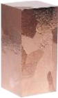
- Sputtering target (Ta)
The melting processes enable us to provide sputtering targets with purity of 6N (99.9999%), well above the industry standard.
-
- Typical Product Application -
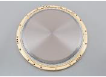
- Low α Sn
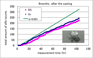
Metal impurities contained in Sn, especially Pb, which is an α-ray emitting element, can be reduced (Pb<0.1 ppm).
Rolling
- Our products extend from rolled copper foil, made using the world’s only integrated production system starting from the copper resource development stage, to sputtering targets made from the ingot stage.
- Ultra-thin foils, ultra-hard foils, and high-performance foils are manufactured through precise control of rolling conditions on different rolling mills, each with its own distinctive features.
- For rolled copper foil, we offer a wide lineup of foil thicknesses, including a very thin 6 µm foil.
-
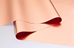
- Typical Product Application -
- Rolled copper foil
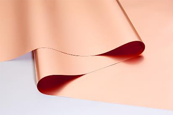
We use integrated process management to manufacture ultra-thin, flat rolled copper alloy foils, incorporating our original expertise and making use of custom-made rolling mills and annealing processes.
-
- Typical Product Application -
- Copper Titanium foil material with high-precision thickness
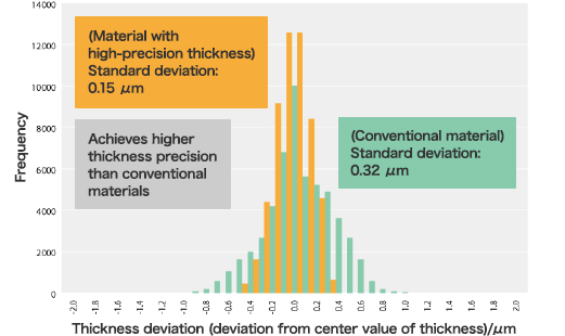
Copper Titanium, one of the hardest copper alloys, is rolled to produce a foil with a thickness of 30 μm. The thickness deviation is only around ± 0.2 μm, well below the tolerance of 1% or less.
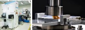
Accurate Bulk Machining
- We use a multi-wire saw for high production efficiency.
- Used with technologies for slicing, grinding, and crystal orientation measurement, this provides extremely flat compound semiconductors.
- Typical Product Application -
- InP substrate

We provide extremely flat substrates matched to the exposure precision demanded in the photolithography process.
Design of metals, alloys, and composites
- Based on the manufacturing know-how and simulation technology we have developed over many years, we study alloy composition and crystal structure, and combine our proprietary rolling and annealing process technologies to achieve the required properties.
-
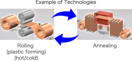
Alloys are produced by repeated processes of rolling and annealing. The size and orientation of the crystal grains are controlled by optimizing the rolling and annealing conditions.
-
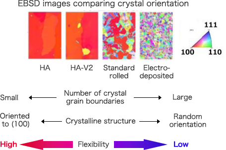
Optimizing the chemical composition and controlling the rolling and annealing conditions enables us to control the size and orientation of the crystal grains and greatly improve flexibility.
Ceramic Material Control
- In the manufacture of ceramic materials, we are able to control grain size by performing all the processes in-house, starting from raw materials.
- Merging each of these technologies (e.g., forming methods, sintering methods, and sintering conditions), we develop high-quality ceramics with distinctive properties.
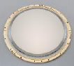
- Typical Product Application -
- Rotary IGZO target

IGZO (In-Ga-Zn-Oxide) targets are used in manufacturing transparent semiconductors for the displays of smartphones and other devices. We provide both planar and rotary targets suitable for the customer's equipment.
Single Crystal Growth
- Applying technologies for high purification, material composition control, and temperature control, we manufacture high-quality single crystals for compound semiconductors.
- In the crystal growth stage, we optimize the growth conditions and temperature profile to manufacture compound semiconductor ingots with large diameter, few crystal defects, and uniformly distributed dopant concentration, providing high-quality compound semiconductor substrates.
-
- Typical Product Application -
- CdZnTe single-crystal substrate
A compound semiconductor substrate being studied for use in infrared and radiation detectors. Along with the world’s largest size, it boasts high quality including uniform in-plane concentration distribution of the Zn additive.
-
- Typical Product Application -
- InP single crystal ingot and single crystal substrates
We provide high-quality compound semiconductor substrates for optical communications.
Powder Manufacture
- Using various grain manufacturing technologies such as breakdown and buildup, we can propose materials suitable for your application.
- Our surface treatment technologies fit your needs, including addition of special features.
Powder Handling
- Features such as grain size, grain distribution, granulation and dispersibility of metal, oxide, and other powders are controlled to realize properties for different applications.
-
- Application -
- Sputtering Targets (W)
Various powder production processes suitable for the final product, such as high purity (5N) sputtering targets.
-
- Application -
- Copper Powder for Additive Manufacturing
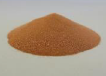
The surface treatment adds an anti-oxidization effect and prevents an increase in the oxygen content, which inhibits AM processing.
-
- Application -
- Sintering copper fine powder

A sintering copper powder with proprietary surface treatment technology, designed to enable both low- and high-temperature sintering depending on the application.
-
- Application -
- Printed Electronics Copper ink

A sintering copper ink with low resistivity,excellent printability, andstrong adhesion fordiverse wiringapplications.
- Technology Employed -
- pulverization/granulation/classification
For a variety of processes: pulverizer, dispersion improver, etc.
Polishing, Etching, and Cleaning
- We process materials such as sputtering targets and compound semiconductor substrates to provide the required properties, from surface roughening by etching to mirror finishing.
- Technology Example -
- Chemical Mechanical Polishing
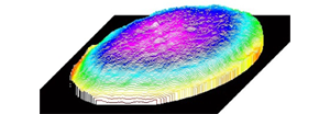
100 mm diameter InP wafer with
thickness deviation of 0.92 μm
Optimizing the balance between the dissolving effects of chemicals and the effects of mechanical abrasion, we create highly flat surfaces with minimal damage.
Surface Deposition and Plating
- We possess technologies for both electrolytic and electroless plating, and capability for high-precision plating at the micron level with either method.
- We carry out consignment business for electroless plating on semiconductor wafers.
Surface Treatment
- Achieves a high-performance plating film by combining plating solutions and post-treatment agents, process technology, analysis and evaluation technology, and simulation technology we have developed in-house.
- Example of Surface Treatment Technology -
- Sealing treatment for gold-plated film
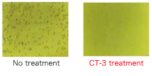
Pit corrosion can be prevented even in corrosive gas by forming an organic treatment film with thickness of approximately 2 nm on the surface of gold-plated film.
- Typical Product Application -
- Copper Foil with BHM Treatment
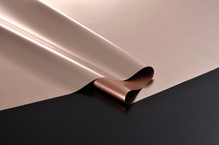
Performance of BHM Treatment for
High-Speed Transmission
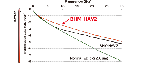
Our surface treatment technology has achieved low transmission loss at high frequency bands while maintaining high peel strength, as well as improving surface flatness.
Adhesion, Bonding, and Compositing
- Uniform bonding strength is achieved by technology suited to each kind of material, such as use of solder or diffusion bonding between different materials. We carry out thorough process control from surface finishing to dimension control.
- Example of Adhesion, Bonding, and Compositing Technology
Before sputtering targets are shipped, they are attached to a base, normally a backing plate or backing tube, for attachment to the sputtering equipment. Since that bond must be of extremely high quality, technology suited to each kind of material is applied, such as use of solder or diffusion bonding between different materials.
Inorganic & Organic Analysis
- Advanced analytical technology is essential for high-performance, high-quality materials
- Examples of Inorganic & Organic Analysis
We have introduced the latest ICP-MS system, ICP-MS/MS, which is less subject to interference by coexistent elements than earlier systems.
We have the largest collection of GDMS six equipment in Japan. This equipment supports our development of high-purity materials by measuring the amounts of trace impurities.
Surface Analysis and Structural Analysis
- We observe and analyze materials using the latest equipment, including devices for scanning electron microscopy (SEM), scanning transmission electron microscopy (STEM), mineral liberation analysis (MLA), X-ray photoelectron spectroscopy (XPS), and auger electron spectroscopy (AES).
- Examples of Surface Analysis and Structural Analysis Technology
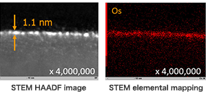
This is an example of analyzing osmium vapor deposited film formed on a silicon substrate at the 1 nm level. With STEM, even ultra-thin films of 1 nanometer can be analyzed.
We utilize ultra-high resolution of 1 nm to investigate the structure of compound semiconductors and sputtered films, and clarify the function expression mechanisms of advanced functional copper alloys.
In-house Evaluation
- We ensure that the expected functions and properties are present in the final form.
- Examples of Technology for Evaluation in Actual Usage Environment
We confirm sputtering performance and thin film properties in order to improve target quality and performance.
We perform bending tests under actual FPC usage conditions to confirm that our copper foils can fulfill bending requirements.
Computer-Aided Engineering and Materials Informatics
- Besides having our own simulation and data analysis technologies,
we also collaborate with outside companies and research institutions to enhance those technologies. Computer science technologies are helping us to design new alloy compositions and improve quality.
- Example of Computer-Aided Engineering
We can conduct comprehensive searches for alloy compositions of three elements, and of four or more elements, thereby speeding up development and ensuring product implementation.
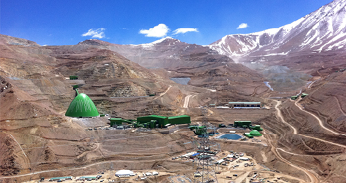
Mineral Resource Exploration and Development
- We are invested in world-leading copper mines, including the Caserones Copper Mine, in which the Group owns a partial interest. Equity copper production volume for fiscal 2020 totaled approximately 200,000 tons, contributing to the stable supply of copper resources.
- In addition, we will invest in rare metal mines, since demand for advanced materials is expected to expand in the future. We are actively working on research and development to this end.
- Caserones Copper Mine
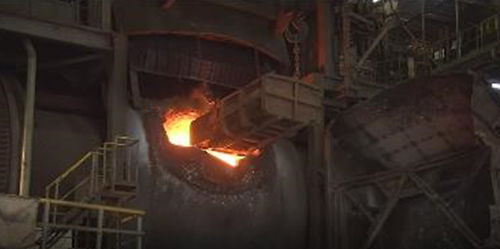
Smelting and Refining
- We have a number of independently developed processes such as a concentrate burner and a wet gold and silver process incorporating a solvent extraction method. Our other uniquely developed processes include pyrometallurgy using a concentrate burner and hydrometallurgy using a solvent extraction method.
- We smelt copper concentrates from overseas mines, including our own mines, and recycled raw materials from urban mines at the same time to stably supply 4N (purity 99.99%) electrolytic copper, precious metals, rare metals, sulfuric acid, etc.
- We are working to reduce CO2 emissions in the smelting process through methods such as using electricity derived from renewable energy and generating power by recovering waste heat from processes.
- Copper Smelting
- (revolving furnace)
Recycling
- Efficient recovery of copper, precious metals, rare metals, etc. from recycled raw materials such as scrapped electrical parts.
- For industrial waste, we implement zero-emission detoxification treatment that does not generate secondary waste.
- Trials are under way for closed recycling of in-vehicle LiBs.
-
- JX Metals Circular Solutions (Tsuruga)
-
- LiB recycling bench scale equipment (Hitachi)