

Printed Electronics Copper ink
Product Overview
- As a sintering material type, it exhibits low electrical resistivity and high thermal conductivity.
- Excellent printability enables the formation of highly linear printed wiring patterns and uniform coated surfaces.
- Outstanding adhesion to various substrates.
- Low resistivity can be achieved at low temperatures under controlled atmospheres such as nitrogen or superheated steam, etc.
- Because we develop and manufacture copper raw materials, copper powders, and copper inks in‑house, we maintain a robust supply chain and can design products tailored to customer requirements.
Copper ink Overview
Key Features of Copper ink
- Low‑resistance wiring can be formed by low‑temperature sintering under a nitrogen or superheated‑steam atmosphere.
Representative conductivity of Copper ink
| Sintering condition | 200℃/ 30 min | 230℃/ 30 min | 200℃/ 30 min |
| Atmosphere | N2 | N2 | Superheated steam |
| Sheet resistivity | 4.9 mΩ/□ (23.6 µm thickness) | 3.6 mΩ/□ (18 µm thickness) | 8.4 mΩ/□ (9.1 µm thickness) |
| Volume resistivity | 11.4 μΩ·cm | 6.4 μΩ·cm | 7.6 μΩ·cm |
Printability of Copper ink
- Enables formation of copper fine‑line patterns with L/S = 10/10 µm by screen offset printing—beyond the capability of screen printing.
- As a fully additive, etch‑free and plating‑free process, it helps to reduce environmental impact.
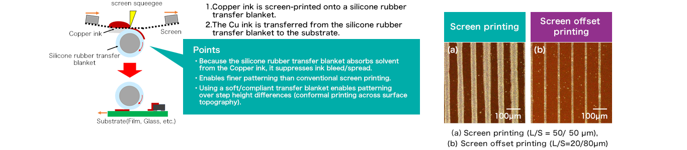
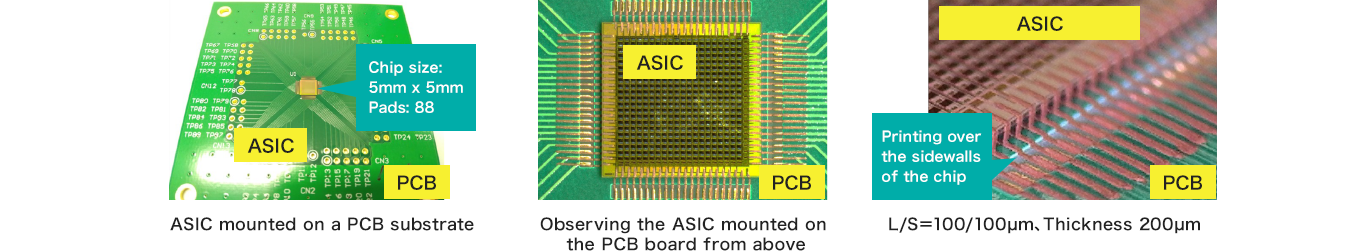
- Screen‑offset printing enables L/S = 100/100 µm printed wiring across a 200 µm step height—unachievable with conventional screen printing.
Copper ink adhesion
- Exhibits strong adhesion to common flexible substrates.
Test conditions
Substrate: polyimide (PI)
Sintering: 250 °C for 30 min under a nitrogen atmosphere
Cross‑cut (crosshatch) adhesion test: in accordance with JIS K 5400‑8.5 (JIS D 0202)
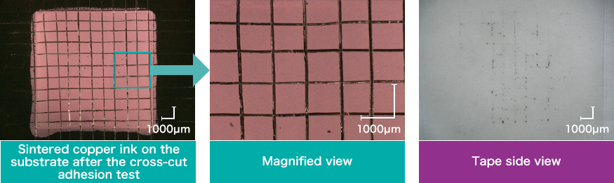
Adhesion classification: 0 (good adhesion)
High‑Frequency Performance
- Sintered copper obtained from the copper ink suppresses transmission loss even at high frequency.
It is promising for applications where interconnect transmission loss at high frequency is a critical challenge.
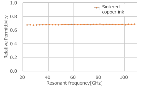
Relative conductivity from resonant frequency measurement using a Fabry–Pérot resonator
(DC four‑probe volume resistivity of the sintered copper from copper ink: 6.0 µΩ·cm).
Frequently Asked Questions (FAQ)
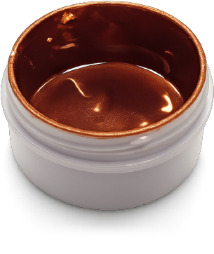
In what supply forms is the product available?
-
We can supply it in syringes and ointment jars, as well as other forms upon request.
What printing method do you recommend?
-
We recommend dispenser printing or screen printing. However, we can also tailor the ink and support other printing methods to meet customer specific requirements.
Other products related to High-Functional Materials for Next Generation Devices
- High-Purity Metals
- Low α Tin/Bismuth for Soft Error Reduction
- Electroless UBM Formation Service
- Compound Semiconductor Wafers - InP, CdZnTe -
- Rutile Single Crystals(Furuuchi Chemical)
- Strontium Titanate Single Crystals(Furuuchi Chemical)
- YAG Ceramics for Laser Applications
- Tantalum and Niobium Oxides and Compounds (TANIOBIS)
- AMPERTEC® High-Purity Chlorides(TANIOBIS)
- Photocatalyst for Artificial Photosynthesis
- Sintering Copper Fine Powder