
Compound Semiconductor Wafers
- InP, CdZnTe -
Summary
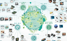
Compound semiconductor substrates (InP) are becoming highly important with the increase in internet communication volume and speed, etc. available in many places. With the arrival of the IoT society, demand is expected to continue to grow.
Application Examples
Features of JX’s InP Wafer
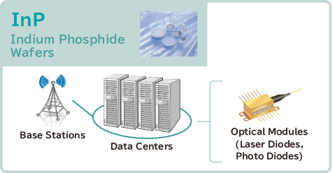
- InP single crystal wafers are used as materials for laser diodes and photo diodes in the optical telecommunications industry.
- We provide high-quality InP single crystal wafers that have achieved the top share of the global market.
- Our technology, including high accuracy of processing as shown right side,contributes to high performance in customer devices.
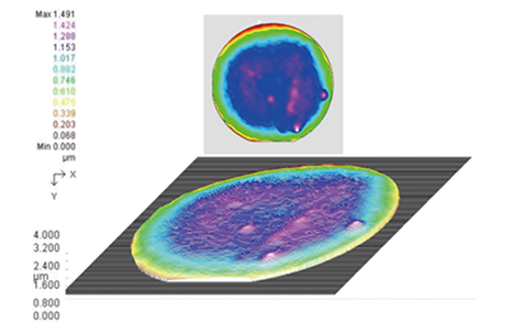
*Total Thickness Variation
New Application Examples by using InP
-
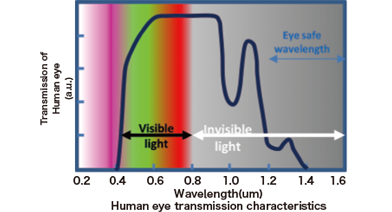
High-performance collision prevention sensor

-
Achieving laser radar at eye-safe
Features of JX’s CdZnTe Wafer
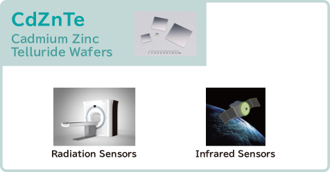
- High quality, large-diameter CdZnTe single crystals are available.
- CdZnTe single crystals are essential for high-sensitivity radiation detectors.
- Our CdZnTe single crystals with highly uniformed Zn concentration enable customers to produce larger module of Infrared sensor.

Compound Semiconductor Materials Product Lineup
| InP | Size | Orientation | Dopant |
|---|---|---|---|
| 2inch 3inch 4inch | (100) | S, Sn, Zn, Fe, None |
| CdZnTe | Size(mm) | Orientation | Dopant |
|---|---|---|---|
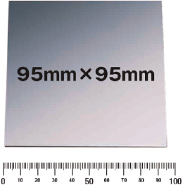
| 10×10- 95×95 | (111),(211),(100) | Zn, None |
FAQ
-
Can you provide examples of introduction?
-
We have a record of sales to customers worldwide spanning more than 40 years.
-
What are the differences from other companies' products?
-
- Optimization of morphology after epitaxial growth By optimizing the plane orientation of the substrate, we have achieved optimization of the surface morphology after epitaxial growth.
- Crack prevention after back surface processing By optimizing the substrate edge shape, it is possible to prevent the edge from cracking during the backside processing process when creating devices.
Other products related to High-Functional Materials for Next Generation Devices
- Printed Electronics Copper ink
- High-Purity Metals
- Low α Tin/Bismuth for Soft Error Reduction
- Electroless UBM Formation Service
- Rutile Single Crystals(Furuuchi Chemical)
- Strontium Titanate Single Crystals(Furuuchi Chemical)
- YAG Ceramics for Laser Applications
- Tantalum and Niobium Oxides and Compounds (TANIOBIS)
- AMPERTEC® High-Purity Chlorides(TANIOBIS)
- Photocatalyst for Artificial Photosynthesis
- Sintering Copper Fine Powder