
A New Contact Method
by Metal Nanowire
(NanoWired GmbH)
Summary
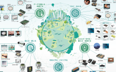
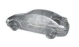
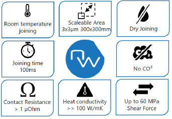
NanoWired is a new expert in joining. The company’s core technology is an unprecedented joining method for the electrical and electronics industries based on NanoWiring structures: cold, fast, and flexible, with ideal thermal and mechanical contact. NanoWired reduces production costs through faster processes, with lower capex and minimization of environmental pollution. The copper-based NanoWired contact eliminates the limitations of soldering, silver sintering, wire bonding, anisotropy gluing, bonding of hybrid material/wafers, welding, and laser welding. NanoWired addresses 2D and 3D packing in the semiconductor industry, shrinking of applications like microLED and IoT, loss-free energy transmission for frequency converters, and heatsink cooling without thermal resistance. Durability is not affected by thermal cycling, power cycling, moisture-heat stress, or thermal storage.
Application Examples
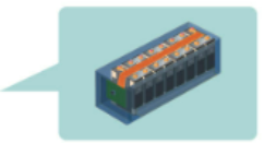
Customer Merits
- Nanowire boding surfaces can achieve interface-free metal-to-metal bonding, resulting in low power consumption at the bonding surfaces.
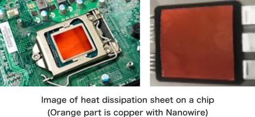
- The Nanowire bonding surfaces can be flexibly adhered to the shape of the surface, and can be used as a heat conductor with excellent thermal conductivity(>>100W/mK).
- In addition, the Nanowire technology has the advantage of improving product performance and production efficiency.
- Possible for boding at room temperature
- Possible for sinter boding at low temperature
- Possible to shorten process time
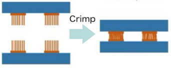
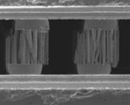
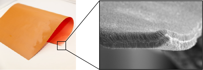
Example of Nanowire bonding (Klettwelding)
Features of NanoWire
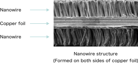
- NanoWired GmbH uses its own technology to generate nanowires (capillary metal) on the surface of copper foils and substrates.
- Currently copper is the main material, but the technology can also be applied to other metals that can be plated because it is an application of a plating technology.
FAQ
What are the advantages of Nanowire technology?
-
Nanowire bonding surfaces can achieve interface-free metal-to-metal bonding, resulting in low power consumption at the bonding surfaces.
The Nanowire bonding surfaces can be flexibly adhered to the shape of the surface, and can be used as a heat conductor with excellent thermal conductivity.
In addition, the Nanowire technology has the advantage of improving product performance and production efficiency.
Are Nanowire samples available?
-
Yes. Please contact NanoWired GmbH directly or via JX Nippon.
In addition, if you need further technical information, please see the FAQ section of the NanoWired GmbH website.
What are the standard process definitions?
-
1. NanoWiring: creates a metallic “lawn” on any surface.
2. VelcroWelding (KlettWelding): enables the joining of two substrates prepared with NanoWiring.
3. Hook-and-loop sintering (KlettSintering): enables bonding with only one substrate prepared with NanoWiring.
4. VelcroGlueing (KlettGlueing): enables adhesive contact between fragile components.
5. VelcroWelding tape (KlettWelding tape): enables even untreated substrates to be joined.
Other products related to Thermal Solutions
- Negative Thermal Expansion Material: ZrW2O8
- Via Filling Paste for Thermal Release / Low Specific Resistance and High Reliability Ag Bonding Wire (TATSUTA Electric Wire and Cable Co., Ltd.)
- Lotus Metal with High-efficiency Heat Radiation(Lotus Thermal Solution)
- Magnetocaloric Spheres for Hydrogen Liquefaction Magnetic Refrigerator